What are the Commercial Applications for Photonic Integrated Circuits?
PICs are already incorporated into the communication backbone of our digital world in the form of data center interconnection and are poised to revolutionize many more applications and industries.
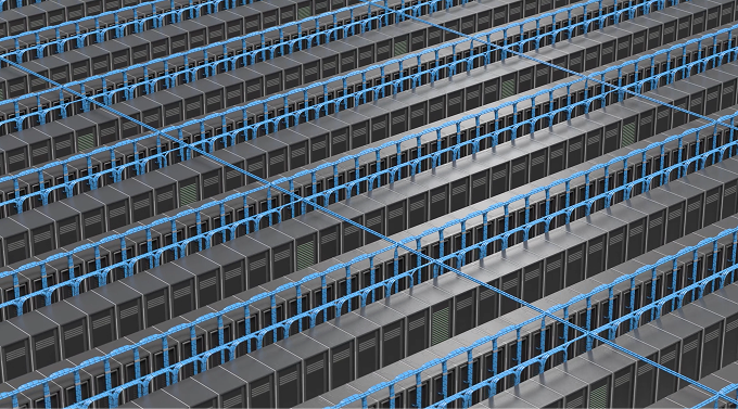
- Where are PICs used today? From the internet’s core infrastructure to hyperscale data centers, PICs are crucial for high-speed, high-bandwidth connectivity, enabling the seamless flow of information that defines our modern lives.
- How can PICs improve cloud computing and AI? By drastically reducing energy consumption and latency while enabling faster data transfer across massive computing infrastructures, PICs are fundamental to scaling cloud services and accelerating AI workloads.
- What other industries benefit? The applications of PICs are vast and growing, spanning autonomous vehicles (LiDAR), quantum computing, biosensing, advanced telecommunications, and high-performance computing.
What are the Benefits and Challenges of Photonic Integrated Circuits?
Key Benefits:
- High Bandwidth at Long Reach: PICs enable data transfer speeds and distances far beyond the capabilities of traditional electrical interconnect, crucial to meet the growing demands of frontier AI models and next gen AI infrastructure.
- Lower Heat and Energy Consumption: The inherent efficiency of light-based communication translates to significantly reduced power consumption and heat dissipation, leading to more sustainable and cost-effective computing.
- Scalable for Next-Gen Computing Needs: As computational demands continue to grow, PICs offer a scalable solution for building larger, more powerful, and more interconnected computing systems.
Key Challenges:
- Performance Stability: Maintaining stable performance across varying environmental conditions is crucial. This includes ensuring consistent operation in the presence of:
- Polarization Changes: The performance of some photonic devices can be sensitive to interactions affecting the polarization state of light, such as power surges or physical handling of fiber optic cables. Designing PICs that are polarization-insensitive or manage polarization effectively is a key to implementation of PICs for high-performance interconnect applications.
- Temperature Variations: Photonic components can be highly sensitive to temperature changes, which can alter their optical properties and affect performance. Robust thermal management and compensation techniques are essential for reliable operation in diverse environments.
Learn More: Passage Technology Breakthrough Performance
- Fiber Attach and Packaging: Efficiently coupling optical fibers to the nanoscale waveguides on a PIC is a significant engineering challenge. Achieving low-loss, high-density, and robust fiber attach solutions is critical for practical deployment and mass production. For advanced applications where the PIC is used as an active interposer (e.g., connecting multiple chips optically within a single package), optimization of advanced packaging techniques is essential. This includes precision alignment of optical interfaces, managing thermal expansion mismatches, and ensuring signal integrity across heterogeneous integration.
- Heterogenous Electronic Integration: Seamlessly integrating photonic components with established electronic systems is a complex engineering task, which the most experienced ecosystem players in silicon photonics have been successfully working through over the past decade. This includes:
- CMOS Integration: Integrating photonic devices with standard Complementary Metal-Oxide-Semiconductor (CMOS) electronic circuits on the same chip or package presents significant challenges. This involves reconciling different material properties, fabrication processes, and thermal management requirements to ensure optimal performance for both optical and electrical functionalities.
- ASIC Integration and Packaging: The integration of optics inside leading edge AI compute and switch chip packages involves more complex integration and test processes, which the largest foundries and Outsourced Semiconductor Assembly and Test (OSAT) vendors have been investing heavily in.
- ASIC Integration and Packaging: The integration of optics inside leading edge AI compute and switch chip packages involves more complex integration and test processes, which the largest foundries and Outsourced Semiconductor Assembly and Test (OSAT) vendors have been investing heavily in.
Learn More: Passage Manufacturing, Packaging and Fiber Attach Technologies
What Is the Future of Photonic Integrated Circuits?
Photonic Integrated Circuits (PICs) are not new—they’ve been deployed for years in telecom and specialized optical systems—but they are still early in their adoption within mainstream data center and AI interconnect applications. As these environments push the limits of electrical interconnects, PICs are emerging as a key enabler of scalable, energy-efficient communication and computation.
3D Integration and Multi-Reticle PIC Interposers
The next stage of PIC deployment centers on 3D integration, where photonics and electronics are vertically stacked to minimize interconnect distance and maximize bandwidth density. PICs will be increasingly being used as optical interposers, serving as high-bandwidth bridges between compute and memory dies.
As these interposers expand beyond a single reticle, cross-reticle stitching enables large multi-reticle PICs—optically connecting wafer-scale or massive complexes of electronic dies with ultra-low latency and high efficiency. This architecture eliminates shoreline constraints and unlocks true system-level optical connectivity.
Expanding Role in AI and Data Center Systems
As AI workloads continue to grow in scale and interconnect demands surge, PICs will become integral to data movement and scaling efficiency across training clusters and inference systems. Their ability to handle massive bandwidth with low power consumption makes them especially valuable for next-generation GPU, TPU, and memory interconnects.
Photonic Computing
The first generation of photonic computers will be very likely hybrid systems, combining the complementary strengths of photonics and electronics within a single package or substrate. As seen in early prototypes, photonic tensor cores perform ultra-high-bandwidth analog operations (such as matrix multiplication), while CMOS circuitry handles digital signal processing, analog-to-digital conversion, control logic, and memory access. This hybrid design exploits the parallelism and bandwidth of light alongside the precision and flexibility of mature CMOS electronics.
Learn More: A New Kind of Computer
Ongoing Research and Innovation
Continuous progress in materials, packaging, and design automation is accelerating the manufacturability and cost-effectiveness of PICs. Research is now focused on improving integration density, thermal management, and reliability, ensuring that photonics can scale seamlessly alongside advanced logic and memory technologies.
Can Photonic Integrated Circuits Enhance Future Consumer Devices?
Yes. As production becomes more scalable and the technology matures, PICs are emerging in consumer tech such as VR/AR devices, where they enable faster, more energy-efficient data transfer and processing, which is crucial for delivering immersive experiences, high-fidelity content, and advanced computational capabilities directly to the user.
Photonic Integrated Circuits and Lightmatter
At Lightmatter, we are at the forefront of this revolution, developing innovative photonic solutions that are already shaping the backbone of today’s and tomorrow’s technologies.
Explore how Photonic Integrated Circuits are merging light and logic for a faster, smarter world with Lightmatter.
Learn More:
Passage L-Series 3D Co-Packaged Optics
Learn how 3D photonic interconnect can accelerate your AI infrastructure: Contact Us