What is a photonic integrated circuit?
Although light does not propagate faster than electrical signals in typical interconnect media, photonics enables much higher bandwidth density, lower signal loss over longer distances, immunity to electromagnetic interference, and lower power and thermal overhead—all of which are critical to scaling AI and other compute-intensive workloads.
How Do Photonic Integrated Circuits Differ from Traditional Integrated Circuits?
Photonic integrated circuits (PICs) use light (photons) to transmit information, whereas traditional integrated circuits use electricity (electrons), enabling faster signal propagation. Although optical signals do not propagate faster than electrical signals in typical interconnect media, photonics enables much higher bandwidth density, lower signal loss over longer distances, immunity to electromagnetic interference, and lower power and thermal overhead—all of which are critical to scaling AI and other compute-intensive workloads.
How Does a Photonic Integrated Circuit Work?
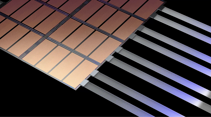
A photonic integrated circuit (PIC) integrates dozens to thousands of miniaturized optical components—such as waveguides, modulators, and detectors—onto a single chip. These components work together to guide, modulate, and detect light, enabling high-speed data transmission and processing at the scale of nanophotonics.
How Are Photonic Integrated Circuits Built?
- Integrated Optical Components: Photonic integrated circuits (PICs) combine key photonic building blocks—like waveguides, modulators (such as microrings or Mach-Zehnder structures), and photodetectors—onto a single silicon or indium phosphide chip.
- Nano-Scale Photonics: Photonic integrated circuits (PICs) leverage nanophotonics—so called because their waveguides are typically only a few hundred nanometers wide and height. This enables the integration of photonic elements like microrings or gratings that are often just microns in size, allowing hundreds of optical functions to operate in parallel within a chip the size of a fingernail.
- Semiconductor-Style Fabrication: Photonic integrated circuits (PICs) are manufactured using lithography and etching techniques similar to those used in traditional semiconductor fabs, enabling high-volume, cost-effective production with precise nanoscale patterning of optical features.
Learn More: Passage 3D Photonic Interconnect Technology
How Are Photonic Integrated Circuits Used in Data Centers?
Photonic integrated circuits (PICs) are enabling a progression of capabilities in the data center:
Pluggable Optical Modules
Optical pluggable modules are compact transceivers that convert electrical signals from switches and servers into optical signals for data transmission across racks or between data centers. Some use lithium niobate (LiNbO₃) modulators, which offer excellent power efficiency and signal linearity, but their large footprint and the need to be placed further from the switch ASIC make them less practical for increasingly dense, high-volume pluggable form factors. Indium phosphide (InP)–based pluggables integrate the laser, modulator, and detector on a single chip, enabling high launch power and excellent optical signal-to-noise ratio (OSNR) for long-reach coherent links. However, they face higher DSP power consumption, thermal constraints, and cost.
As data rates scale from 800 Gbps to 1.6 Tbps and beyond, pluggables are transitioning to silicon photonics (SiPho) to enable tighter integration—even within the same package as the GPU/switch. The tighter integration will lead to lower total power, and better thermal efficiency. Traditional pluggables consume more power per bit primarily due to power-hungry coherent DSPs, higher laser power, and electrical I/O overhead—factors that SiPho architectures can significantly reduce at scale.
Photonic (or Optical) Interconnects
As scale-up pods in data centers expand beyond a single rack. PIC-enabled photonic interconnects are expected to replace passive electrical signaling over copper, whose reach limit is roughly one meter at high speeds due to resistive losses and crosstalk. Photonic interconnects enable high-throughput links over distances of millimeters to hundreds of meters at significantly lower power per bit than in pluggable transceivers. This new category of interconnect is implemented Near Package Optics (NPO), Co-Packaged Optics (CPO), or Active Photonic Interposers, where photonics is integrated near or inside the switch or compute chip package. Collectively, these photonic interconnect applications are also referred to as Optical Engines (OE).
Learn More: Charting the Photonic Future of AI Interconnect
Memory and Storage Disaggregation (emerging/future)
As data-hungry AI and HPC workloads grow, tightly coupled compute-memory architectures become a bottleneck. PICs can enable optical memory fabrics using technologies like CXL over optics or optical HBM links, allowing pooled, disaggregated memory and storage with ultra-low latency and massive bandwidth—breaking the limitations of traditional DDR or PCIe buses.
Photonic Computing (future)
Still in the early research stages, photonic computing aims to use light not just for transmitting data but for performing logic and arithmetic operations. PICs are central to this vision, enabling on-chip optical matrix multiplication, Fourier transforms, and signal processing at the speed of light. This could unlock orders-of-magnitude performance gains for AI inference, especially for workloads dominated by linear algebra.
Learn More: A New Kind of Computer
What Problems Do Photonic Integrated Circuits Solve?
For AI Data Center Interconnect
PIC-based interconnects solve the scaling limitations of copper and discrete optics by enabling:
- Wavelength-division multiplexing (WDM) for scalable bandwidth within the same physical link
- Low power per bit (as low as single-digit picojoules), reducing thermal load in AI clusters
- Longer reach (up to kilometers) without signal degradation
- Footprint and cost reduction through high levels of optical integration
Together, these benefits help overcome I/O bottlenecks between GPUs, accelerators, and switches, enabling the high-density fabrics needed for next-gen AI workloads.
For Memory and Storage Disaggregation
PICs solve the bandwidth and latency bottlenecks of traditional electrical memory buses by enabling:
- Low-latency optical links between disaggregated memory, storage, and compute nodes
- High-density optical interconnects that support scalable, rack-level memory pools without the switching hierarchy implicit in CXL standards
- Energy-efficient data movement, crucial as memory access becomes a power bottleneck
- Protocol-agnostic optical transport, supporting standards like CXL
This facilitates a more flexible and efficient data center architecture, where memory and storage can be dynamically allocated across compute resources.
For Photonic Computing
Photonic Integrated Circuits address fundamental compute limitations by:
- Performing computations in the optical domain, bypassing transistor-based bottlenecks
- Enabling parallel, low-latency operations ideal for AI, signal processing, and scientific computing
- Reducing energy per operation dramatically—light doesn’t require charging and discharging gates
- Opening the door to ultra-fast, domain-specific processors that operate at the speed of light
While still in the early stages of its technology lifecycle, photonic integrated circuits could ultimately drive the next exponential advances in AI workloads, where energy and data movement dominate the cost of computation.
Learn More: Lightmatter’s Technology Transforms Next Gen AI Infrastructure