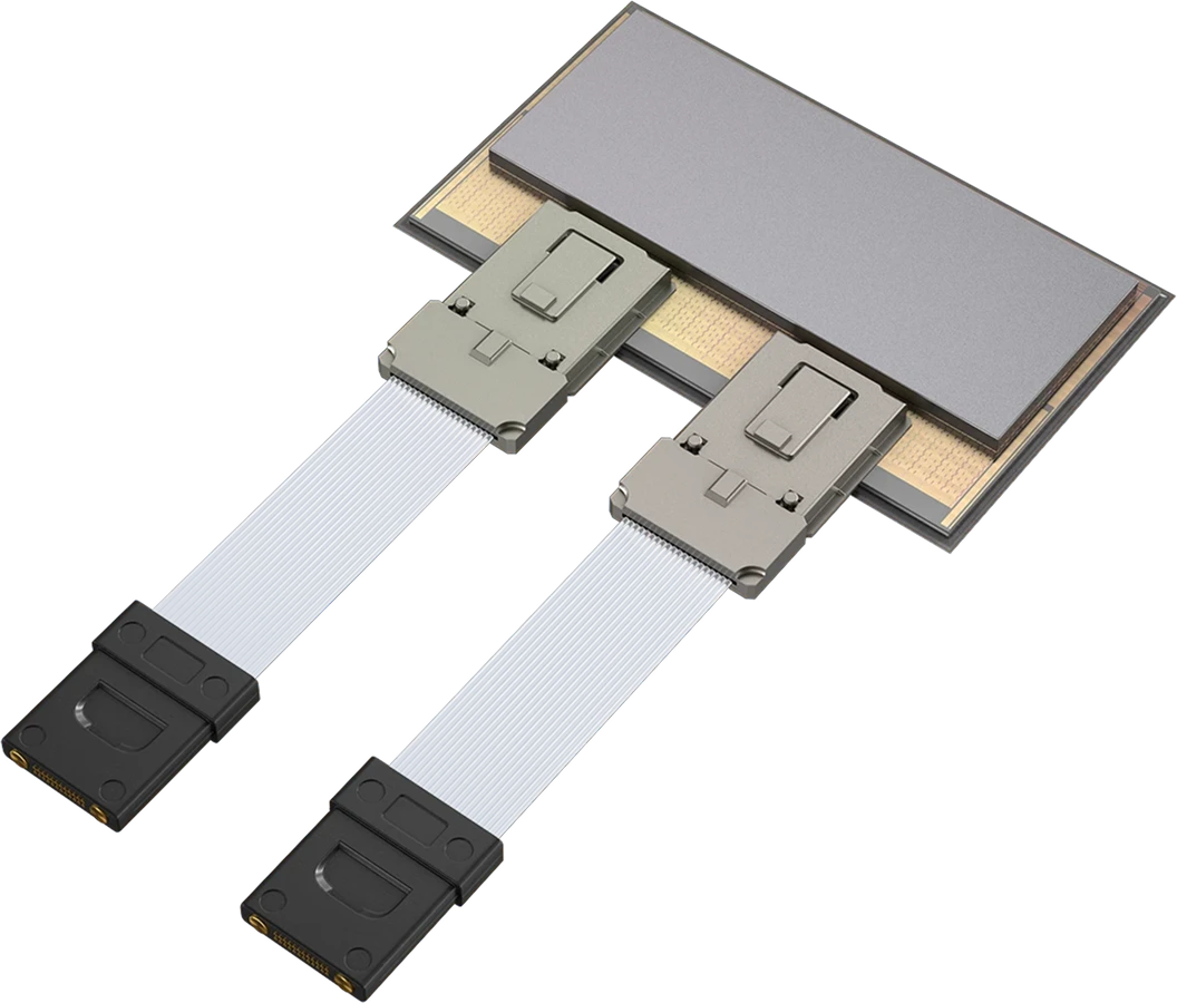
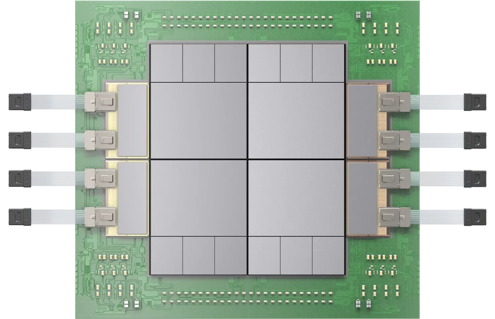
PASSAGE L200

First Edgeless I/O 3D Co-Packaged Optics

Passage L200 eliminates the shoreline bottleneck. By stacking the photonic engine with the electronic IC, we deliver 32-64 Tbps of optical I/O per chip—enabling bandwidth densities 5-10x greater than conventional solutions.

Bandwidth

32-64

Tbps Optical I/O

Total I/O

200+

Tbps / Chip

Density

10x

vs Pluggables

Latency

Linear

Drive Architecture

Architecture

Breaking the Shoreline Constraint

The Challenge

Conventional chip I/O is confined to the die edges (“shoreline”). As die area scales (r²), perimeter scales only linearly (2πr), creating a bandwidth bottleneck. Chips exhaust edge space long before they exhaust compute capability.

The L200 Solution

Passage removes this constraint by vertically integrating the photonic IC (PIC) beneath the electronic IC (EIC). This allows SerDes and optical interfaces to be placed across the entire die surface, enabling bandwidth density that scales with silicon area rather than die perimeter.

Technical Specifications

Optical Bandwidth
32 Tbps (L200) / 64 Tbps (L200X)
Modulation
PAM4 (56G, 112G)
Integration
3D chip-on-wafer (CoW)
Energy efficiency
< 5 pJ/bit (Optical)
Topology
Edgeless I/O (area-array)
Serviceability
Detachable fiber connectors
Direct drive reach
10m to 2km (DR/FR)

Ready to scale?

L200 design partnerships are open for 2026 roadmaps.