Interconnect Is All You Need: Final Nodes, Big Chips, and Photonics
Humanity’s progress has always paralleled advances in computing. From the abacus to the modern computer, each leap forward has not only improved our capabilities but also reshaped the world. Computers are a tool for freeing the mind of monotony, allowing us to focus on the core problem we are solving. The rapid acceleration of these developments over the past few decades has brought us to the brink of something truly extraordinary: the creation of artificial superintelligence (ASI).
The Path to Superintelligence
The belief that ASI may become a reality is not based on science fiction but on a series of pivotal computing events. The advent of digital computers in the mid-20th century, the invention of the transistor, the birth of the Internet, and the exponential growth in data processing power have all set the stage. Each of these milestones has progressively enabled machines to perform tasks that were once the exclusive domain of humans.
Over the last few decades, we’ve seen machines master complex games, interpret natural language, and readily create art. These achievements are not isolated — they are part of a broader trend where computing systems increasingly replicate and exceed human cognitive functions. The acceleration of machine learning, the rise of neural networks, and the vast amounts of data now available have all contributed to the growing belief that ASI is not just possible but inevitable.
Inopportune Timing: Slowing Compute Scaling Laws
It is an oddity of timing that just as we are on the cusp of creating ASI, the traditional methods that have fueled our computing progress are hitting their limits. For nearly five decades, Moore’s Law — the observation that the number of transistors on a microchip doubles approximately every two years — has been the engine driving our computational advancements. This exponential growth (coupled with constant transistor power density, known as Dennard Scaling) has underpinned the increasing complexity and power of our computing systems.
But Moore’s Law no longer holds. Silicon transistors are pushing against fundamental, physical limits, and the rate of progress in traditional silicon-based computing has dramatically slowed. It is increasingly likely that a final process node will exist with the best-known lithographic technology. Beyond this node, the economic cost and performance gain will no longer be commensurate. This slowdown presents a significant challenge at a time when the demand for more powerful computation, particularly for AI applications, has never been greater.
The Promise of Photonics
Enter photonics — a technology that has been around for two decades and is now stepping into the spotlight. Photonics involves using light, rather than electrical signals, typically to transmit data; the technology can also be used for computation. This additional capability may be important later in developing information-processing machines. Leveraging photonics offers the potential for much higher speeds, lower power consumption, and further reach compared to traditional electronics. Photonics outperforms electronics for data transport because photons avoid resistive losses, capacitance, and inductance, eliminating energy storage and delay effects, which allows lower signal attenuation and higher bandwidth over longer distances.
Photonics has emerged at a crucial moment — just as Moore’s Law and Dennard Scaling have faltered. It offers a path forward by enabling the creation of more efficient and powerful computing systems to meet the demands of ASI. This technology promises to extend our computational capabilities far beyond what is possible with today’s silicon-based processors.
Approaching Maximum-Sized Chips
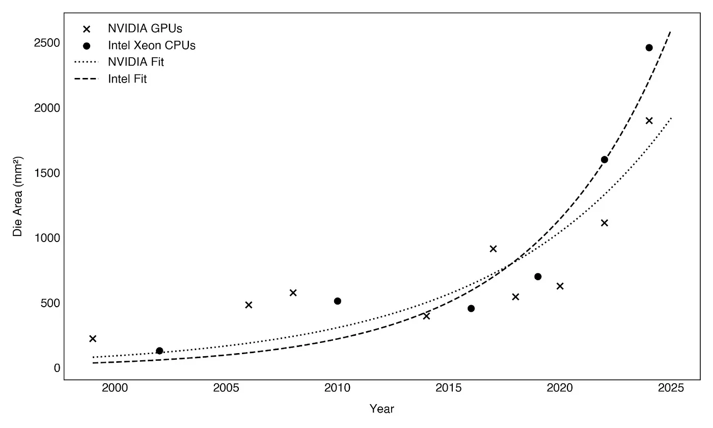
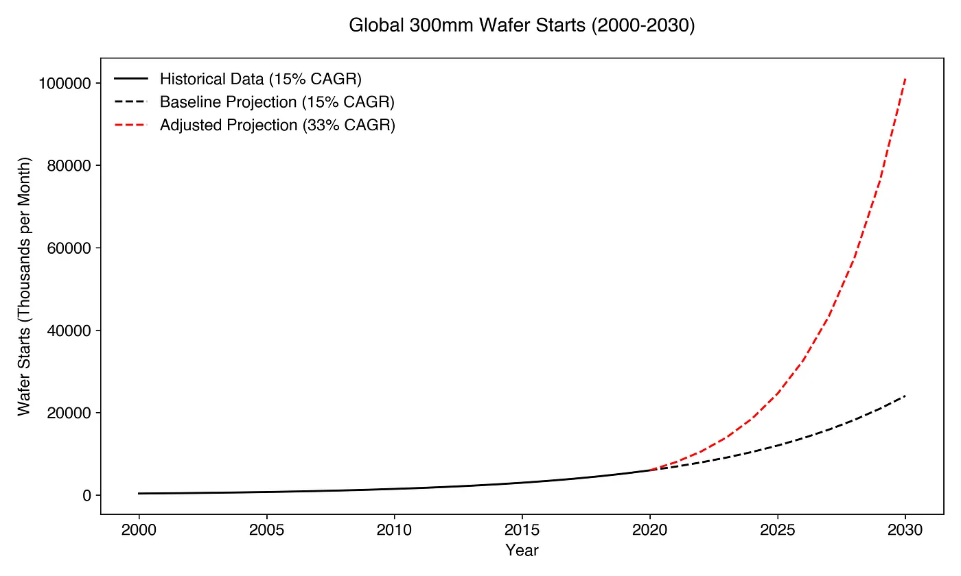
The number of 300mm wafers manufactured at foundries has grown at a 10–15% annual rate over the past two decades. With the death of Moore’s Law and Dennard Scaling, the primary performance scaling vector is exponentially increasing silicon area, as shown in Fig. 1. By fitting this data, we can extract a compound annual growth rate for silicon content per package. This growth rate will compound with that of 300 mm wafer starts (about 10% annually) and potentially cause a dramatic increase in the number of wafer starts, as shown in Fig. 2. At least two companies are already at wafer-scale: Cerebras with their wafer-scale engine and Tesla with Dojo. Beyond this, future work into glass, panel-level substrates would enable “chips” up to (450 mm x 450 mm). Fitting the curve in Fig. 1 predicts that today’s 4000 mm2 data center chips will reach wafer scale (~40,000 mm2) in the next 15 years. Lightmatter’s PassageTM technology supports today’s chip sizes and wafer scale chips.

Growth of silicon die area for NVIDIA GPUs and Intel Xeon CPUs. The fits imply compound annual growth rates of 13% and 18% for NVIDIA and Intel, respectively. Based on these growth rates, we can expect both Intel and NVIDIA to reach wafer-scale somewhere around 2040.

Global 300mm wafer starts from 2000 through a projected 2030. As silicon area per package grows exponentially to meet performance roadmap requirements of AI and the death of Moore’s Law, wafer starts may increase dramatically.
We are approaching the final process node for silicon foundries due to fundamental physical, economic, and technological limitations. As feature sizes approach one nanometer, quantum effects like electron tunneling and leakage currents undermine transistor reliability while increasing power density and heat dissipation challenges limit efficiency gains. The rising costs of fabricating chips at smaller nodes and declining yields make further miniaturization economically unsustainable. Additionally, silicon’s material properties and interconnect bottlenecks restrict further scaling. The decline of Moore’s Law and the shift toward emerging technologies like quantum computing, 3D stacking, and alternative materials signal that silicon’s role in driving performance gains is nearing its limit, and future advancements will likely depend on post-silicon approaches.
As we look to continue our computing journey, the first step (which has already begun) is assembling our final-node chips into a single datacenter-scale computer. This approach involves integrating thousands to millions of advanced chips into a cohesive system that can function as a single, massively powerful computational unit. Such a system would be capable of handling the immense computational demands required for AI and ASI, pushing the boundaries of what is possible today.
Interconnect Topologies for Final Node, Maximum-Sized Chips
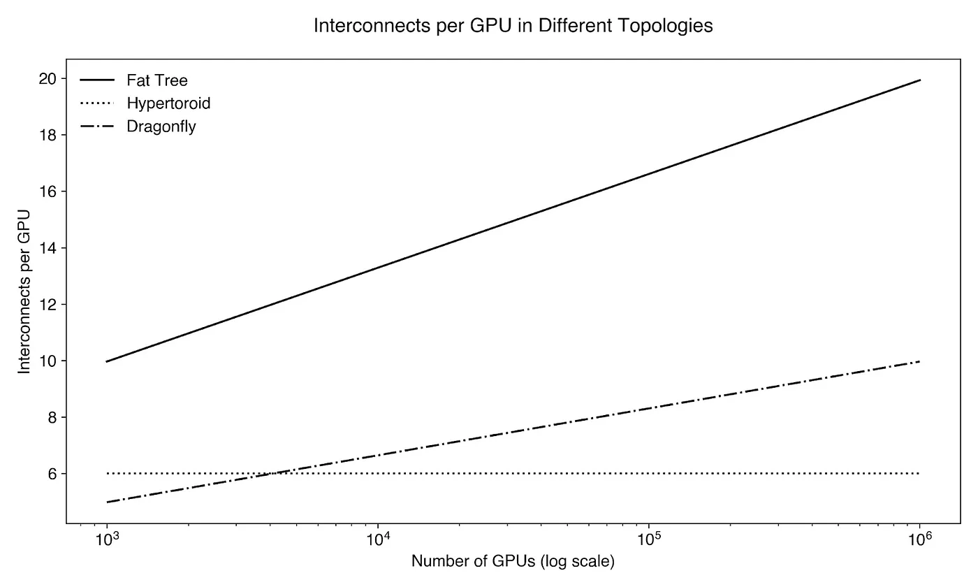
The number of interconnects per AI supercomputer grows rapidly with the number of XPUs. In a fully connected system, where every chip needs to communicate with every other chip, the number of interconnections scales quadratically with the number of chips. This means that even modest increases in the number of chips lead to a disproportionately large growth in the number of interconnections. Practically, large AI clusters are not architected with a fully connected topology. As the number of XPUs increases, the resulting surge in the number of communication links presents significant challenges for routing, bandwidth, and latency. New technologies like Lightmatter’s Passage are needed to enable the radices required to build ultra-high performance networks that minimize the number of layers of packet switches.

Visualization of different interconnect networking topologies. The number of photonic links required to realize each topology as a function of the size of XPU cluster varies significantly — motivating careful selection of topology.

Interconnects per GPU for different interconnect topologies. Each GPU is assumed to have a single interconnect or link. Network topology significantly impacts the performance of an AI workload, and different topologies require different interconnects per GPU. In all cases, the number of interconnects grows with cluster size. There are many more interconnects than GPUs.
At Lightmatter’s founding, we recognized that the technology that scaled computing advancements for the past 50 years was being undone and could not sustain or carry innovation into the next decade. A new kind of scaling surfaced, and we saw — through our unique world lens — the potential of photonics to address it. This recognition led to the invention of Passage, a revolutionary approach to assembling computer chips that leverages photonics as the platform upon which all next-generation computing systems will be built. Passage represents a critical step toward enabling the computational power necessary for the future of AI and whatever comes next.

A Lightmatter-enabled data center. Instead of islands of compute, the entire data center acts as a single computer — maximizing compute performance for training the largest AI models.
Conclusion
Humanity’s progress is tied to our ability to compute. As we stand on the verge of creating ASI, we must confront silicon’s limitations and the traditional scaling laws that have carried us this far. The convergence of slowing silicon advancements and astronomically rising computational demands has brought us to a pivotal moment. We’re nearing the final process node and the only way forward is massive chips. There’s a limit to how big chips can be.
The future of computing is no longer just about processing power — it’s about how we can interconnect arrays of final node, maximum-sized chips. In the AI data centers of tomorrow, the network will dominate. As silicon reaches its physical limits, photonics offers a way forward, enabling systems that are faster, more efficient, and more scalable than anything silicon alone could achieve.
At Lightmatter, we have built the technology that will define the future of computing. Passage enables up to wafer-scale chips and the growing bandwidth requirements of gigawatt AI clusters and introduces fundamentally new capabilities to data centers. With photonics, we will transform how chips are assembled and how data moves in the most advanced AI systems, ensuring that the next chapter of computing is defined by continued innovation and progress.
The path to ASI and beyond will be guided by light.
Nick Harris, PhD
Founder, CEO